A bipolar transistor consists of a three-layer “sandwich” of doped (extrinsic) semiconductor materials, either P-N-P in Figure below(b) or N-P-N at (d). Each layer forming the transistor has a specific name, and each layer is provided with a wire contact for connection to a circuit. The schematic symbols are shown in Figure below(a) and (d).
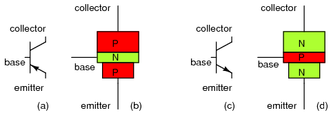
BJT transistor: (a) PNP schematic symbol, (b) physical layout (c) NPN symbol, (d) layout.
The functional difference between a PNP transistor and an NPN transistor is the proper biasing (polarity) of the junctions when operating. For any given state of operation, the current directions and voltage polarities for each kind of transistor are exactly opposite each other.
Bipolar transistors work as current-controlled current regulators. In other words, transistors restrict the amount of current passed according to a smaller, controlling current. The main current that is controlled goes from collector to emitter, or from emitter to collector, depending on the type of transistor it is (PNP or NPN, respectively). The small current that controls the main current goes from base to emitter, or from emitter to base, once again depending on the kind of transistor it is (PNP or NPN, respectively). According to the standards of semiconductor symbology, the arrow always points against the direction of electron flow.

No comments:
Post a Comment